Ion Beam Etching Process
.jpg)
An Introduction To Ion Beam Etching
4wave Ion Beam Etch 4wave Inc

Schematic Drawing Of The Veeco Rf 350 Ion Beam Etching System That Was Download Scientific Diagram

Dry Etch Processes Dryetching Semiconductor Technology From A To Z Halbleiter Org
Ion Beam Etching Cleaning

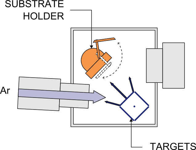
Schematic Of The Ion Beam Etching Ibe System Download Scientific Diagram

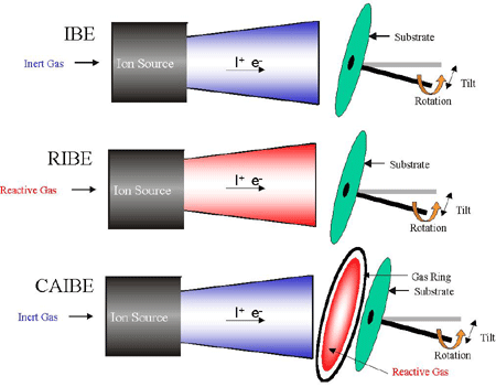
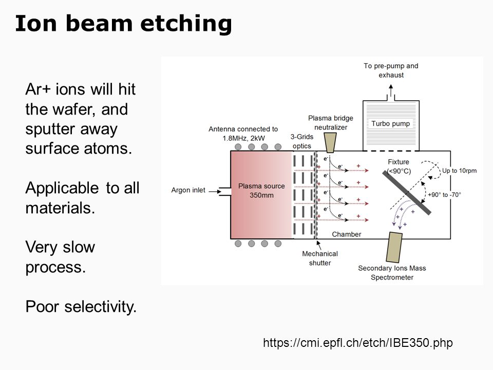
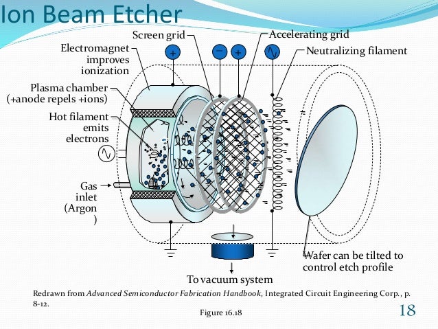
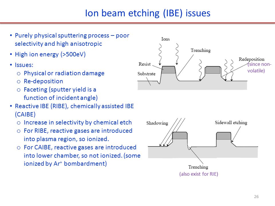
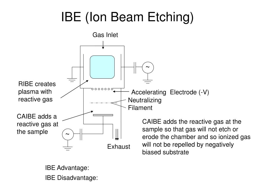
Ibm or etching is generally a surface finishing process in which the material removal takes place by sputtering of ions.
Ion beam etching process.
Etching Chapters 11 20 21 We Will Return To This Topic In Mems Ppt Video Online Download
Etching Processes For Microsystems Fabrication
Material Removal Etching Processes Ppt Video Online Download

Microelectronics Processing Ppt Video Online Download
Ion Beam Etching And Sin Sputtering System Polifab

Reactive Ion Beam Etching Of Large Diffraction Gratings Plymouth Grating Laboratory

Pt Ti Tin And Sio 2 Etch Rates As A Function Of Ion Beam Angle Of Download Scientific Diagram

Focused Ion Beam An Overview Sciencedirect Topics

Ion Beam Technology Nordiko Technical Service Ltd

Introduction To Ion Beam Etching With The Em Tic 3x Learn Share Leica Microsystems
Ion Beam Milling And Etching Systems Nano Master Inc Etching

Ion Beam An Overview Sciencedirect Topics
Https Avs Scitation Org Doi Pdf 10 1116 1 4932161
Http Www Vacuum Uk Org Pdfs Vs7 Vacuumquality Dpearson Pdf
Ppt Lecture 8 Plasma Etching Powerpoint Presentation Free Download Id 243638
Ion Beam Deposition Ibd Oxford Instruments
Https Www Tf Uni Kiel De Matwis Afm Download Mst Ws2018 Dry Etching 2018 Pdf
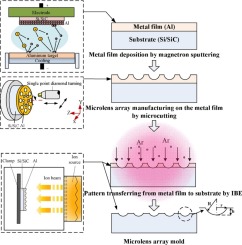
Study On New Method And Mechanism Of Microcutting Etching Of Microlens Array On 6h Sic Mold By Combining Single Point Diamond Turning With Ion Beam Etching J Mater Process Tech X Mol
Https Encrypted Tbn0 Gstatic Com Images Q Tbn 3aand9gctkyivnn8epktleme5f4xlkr5wpejutmda56at8sixj5l8xgart Usqp Cau

Pin Di Beam

Materials Processing Using Radio Frequency Ion Sources Ion Beam Sputter Deposition And Surface Treatment Review Of Scientific Instruments Vol 90 No 2

Non Contact Polishing Of Single Crystal Diamond By Ion Beam Etching Sciencedirect

Pdf Ion Beam Figuring Of Optics

Fine Tuning The Etch Depth Profile Via Dynamic Shielding Of Ion Beam Sciencedirect
Source : pinterest.com
